|
 
- UID
- 1023166
- 性别
- 男
- 来自
- 燕山大学
|

Infineon TC1797 32位TriCore评估方案
Infineon公司的TC1797是采用32位TriCore V1.3.1 CPU的单片微控制器(MCU),具有4级流水线,优异的实时性能,全集成的DSP功能,单精度浮点单元(FPU),全温度范围内(-40° 到+125°C)180MHz或150MHz工作,片内具有多种存储器,高性能片内总线架构和多种外设单元,核电压1.5V,I/O电压3.3V,主要用在汽车和工业系统.本文介绍了TC1797主要特性,方框图和TriBoard-TC179X V5.0评估板主要特性,框图,电路图和PCB元件布局图.
This document is designed to be read primarily by design engineers and software engineers who need a detailed description of the interactions of the TC1797 functional units, registers, instructions, and exceptions.
This TC1797 Data Sheet describes the features of the TC1797 with respect to the TriCore Architecture. Where the TC1797 directly implements TriCore architectural functions, this manual simply refers to those functions as features of the TC1797. In all cases where this manual describes a TC1797 feature without referring to the TriCore Architecture, this means that the TC1797 is a direct implementation of the TriCore Architecture.
Where the TC1797 implements a subset of TriCore architectural features, this manual describes the TC1797 implementation, and then describes how it differs from the TriCore Architecture. Such differences between the TC1797 and the TriCore Architecture are documented in the section covering each such subject.
The TC1797 combines three powerful technologies within one silicon die, achieving new levels of power, speed, and economy for embedded applications:
• Reduced Instruction Set Computing (RISC) processor architecture
• Digital Signal Processing (DSP) operations and addressing modes
• On-chip memories and peripherals
DSP operations and addressing modes provide the computational power necessary to efficiently analyze complex real-world signals. The RISC load/store architecture provides high computational bandwidth with low system cost. On-chip memory and peripherals are designed to support even the most demanding high-bandwidth real-time embedded control-systems tasks.
TC1797主要特性:
• High-performance 32-bit super-scalar TriCore V1.3.1 CPU with 4-stage pipeline
– Superior real-time performance
– Strong bit handling
– Fully integrated DSP capabilities
– Single precision Floating Point Unit (FPU)
– 180 or 1501) MHz operation at full temperature range
• 32-bit Peripheral Control Processor with single cycle instruction (PCP2)
– 16 Kbyte Parameter Memory (PRAM)
– 32 Kbyte Code Memory (CMEM)
– 180 or1501) MHz operation at full temperature range
• Multiple on-chip memories
– 4or 31) Mbyte Program Flash Memory (PFLASH) with ECC
– 64 Kbyte Data Flash Memory (DFLASH) usable for EEPROM emulation
– 128 Kbyte Data Memory (LDRAM)
– 40 Kbyte Code Scratchpad Memory (SPRAM)
– Instruction Cache: up to 16 Kbyte (ICACHE, configurable)
– Data Cache: up to 4 Kbyte (DCACHE, configurable)
– 8 Kbyte Overlay Memory (OVRAM)
– 16 Kbyte BootROM (BROM)
• 16-Channel DMA Controller
• 32-bit External Bus Interface Unit (EBU) with
– 32-bit demultiplexed / 16-bit multiplexed external bus interface (3.3V, 2.5V)
– Support for Burst Flash memory devices
– Scalable external bus timing up to 75 MHz
• Sophisticated interrupt system with 2 × 255 hardware priority arbitration levels serviced by CPU or PCP2
• High performing on-chip bus structure
– 64-bit Local Memory Buses between CPU, EBU, Flash and Data Memory
– 32-bit System Peripheral Bus (SPB) for on-chip peripheral and functional units
– One bus bridges (LFI Bridge)
• Versatile On-chip Peripheral Units
– Two Asynchronous/Synchronous Serial Channels (ASC) with baud rate generator, parity, framing and overrun error detection
– Two High-Speed Synchronous Serial Channels (SSC) with programmable data length and shift direction
– Two serial Micro Second Bus interface (MSC) for serial port expansion to external power devices
– Two High-Speed Micro Link interface (MLI) for serial inter-processor communication
– One MultiCAN Module with 4 CAN nodes and 128 free assignable message objects for high efficiency data handling via FIFO buffering and gateway data transfer
– One FlexRayTM module with 2 channels (E-Ray).
– Two General Purpose Timer Array Modules (GPTA) with additional Local Timer Cell Array (LTCA2) providing a powerful set of digital signal filtering and timer functionality to realize autonomous and complex Input/Output management
• 44 analog input lines for ADC
– 3 independent kernels (ADC0, ADC1, ADC2)
– Analog supply voltage range from 3.3 V to 5 V (single supply)
– Performance for 12 bit resolution (@fADCI = 10 MHz)
• 4 different FADC input channels
– channels with impedance control and overlaid with ADC1 inputs
– Extreme fast conversion, 21 cycles of fFADC clock (262.5 ns @ fFADC = 80 MHz)
– 10-bit A/D conversion (higher resolution can be achieved by averaging of consecutive conversions in digital data reduction filter)
• 221 digital general purpose I/O lines1) (GPIO), 4 input lines
• Digital I/O ports with 3.3 V capability
• On-chip debug support for OCDS Level 1 (CPU, PCP, DMA, On Chip Bus)
• Dedicated Emulation Device chip available (TC1797ED)
– multi-core debugging, real time tracing, and calibration
– four/five wire JTAG (IEEE 1149.1) or two wire DAP (Device Access Port) interface
• Power Management System
• Clock Generation Unit with PLL
• Core supply voltage of 1.5 V
• I/O voltage of 3.3 V
• Full automotive temperature range: -40° to +125℃
• Package variants: P/PG-BGA-416-10
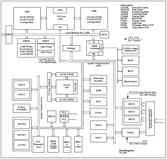
图1.TC1797 方框图
TriBoard-TC179X V5.0评估板
We congratulate you on your purchase of the TriCore Evaluation Board. This kit is a versatile tool, providing quick access to the capabilities of TriCore’s powerful architecture.
Applications can be developed easily. The Evaluation Board is equipped with a variety of memories and peripherals for connection to the environment. There is also an interface for the On Chip Debugging Features (OCDS1 and DAP). The kit also includes several sets of development tools, which are stored on the included Evaluation Board CD-ROM.
The Evaluation Board allows easily the development of TriCore applications with the corresponding tools.
Subsequently, the applications can be downloaded and can be tested with the powerful debugger software.
This TriBoard Hardware Manual familiarizes you with the TriCore Evaluation Board and guides you through the initial configuration of the TriBoard.
TriBoard-TC179X V5.0评估板主要特性:
– Infineon’s TC179X (TC1792,TC1796,TC1797) Controller in PG-BGA416 Package
– Infineon’s TC1793 Controller in PG-LBGA416 Package
– Burst Flash up to 16MBytes
– asynchronous SRAM up to 1MByte
– synchronous SRAM up to 8 MByte
– FlexRay Transceivers (optional if not with TC1797 or TC1793)
– High Speed CAN Transceivers
– USB to UART bridge
– Crystal 20MHz (default), Oscillator or External Clock
– USB miniWiggler JDS for easy debugging
– 8 Low Power Status LEDs
– 8-DIP switches for configuration
– access to all pins of controller
– 100mm x 160mm (EURO-Board)
Connectors
The TC179X TriBoard offers a wide variety of connectors:
– Standard power connector
– USB connector for ASC Interface (ASC0) and miniWiggler
– 16-pin header for JTAG interface (OCDS)
– 10-pin header for DAP (only TC1797 and TC1793)
– 2 x 10pin (2x5) Header for CAN High Speed Transceiver (CAN0 and CAN1)
– 2 x SUB-D9 Plug connector for FlexRay (optional if not with TC1797 or TC1793)
– four 80-pin connectors (male) + four 80-pin connectors (female) with all I/O signals
– optional ETK connector
Components
– Infineon’s Next generation micro controller supply TLE 7368-E (TLE7368-3E for TC1793 if available)
– Three LEDs to validate power supply (5Volt / 3,3 Volt / VCORE)
– LED indicating /HDRST (ESR0) active state
– LED indicating activ miniWiggler JDS
– LED switched via DAS software
– Infineon’s FlexRay Communication Controller SAK-CIC310 (optional if not with TC1797 or TC1793)
– 2x FlexRay Transceiver AS8221(AMS) or TJA1080 (NXP) (optional if not woth TC1797 or TC1793)
– 2 x Infineon’s High Speed CAN-Transceiver TLE 6250 GV33
– USB to UART bridge FT2232HL (FTDI)
– SPI eeprom (Atmel)
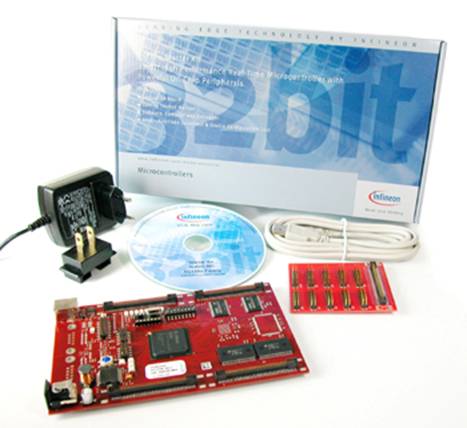
图2.TriBoard-TC179X V5.0评估板外形图
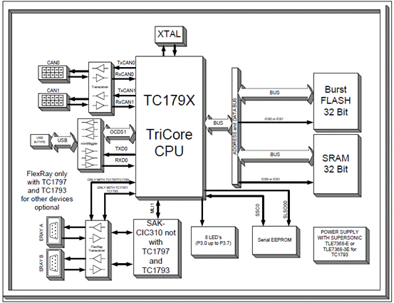
图3.TriBoard-TC179X V5.0评估板框图
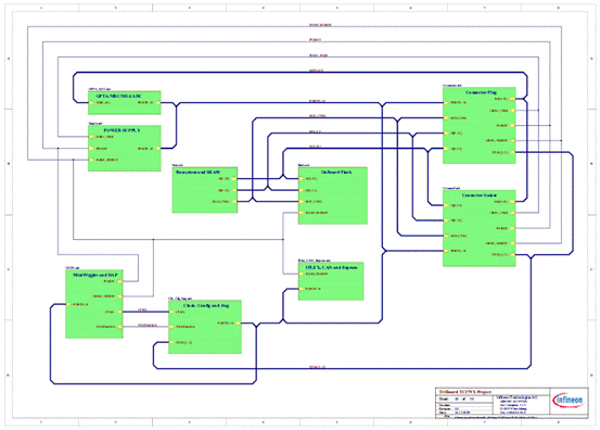
图4.TriBoard-TC179X V5.0评估板项目框图

图5.TriBoard-TC179X V5.0评估板电路图:总线系统和SRAM
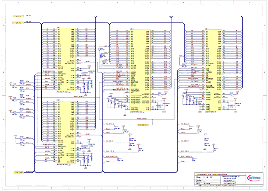
图6.TriBoard-TC179X V5.0评估板电路图:板上闪存
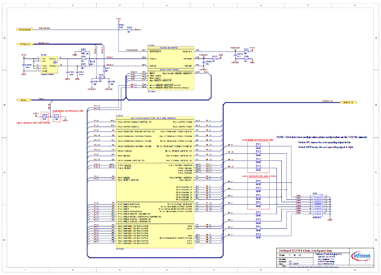
图7.TriBoard-TC179X V5.0评估板电路图:时钟,配置和JTAG
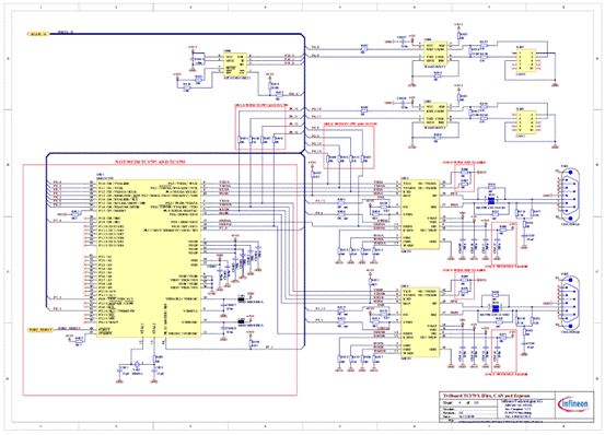
图8.TriBoard-TC179X V5.0评估板电路图: IFlex, CAN和EEPROM
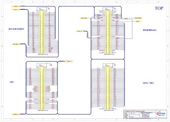
图9.TriBoard-TC179X V5.0评估板电路图: miniWiggler JDS, DAP和ETK

图10.TriBoard-TC179X V5.0评估板电路图: GPTA, MSC, MLI和ADC
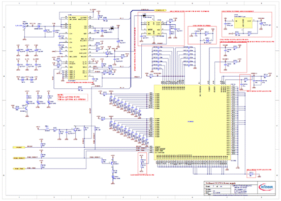
图11.TriBoard-TC179X V5.0评估板电路图:电源

图12.TriBoard-TC179X V5.0评估板电路图:连接器(插头)
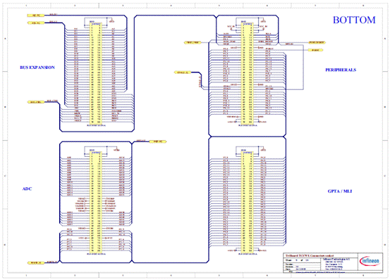
图13.TriBoard-TC179X V5.0评估板电路图:连接器(插座)

图14.TriBoard-TC179X V5.0评估板元件布局图(顶层)
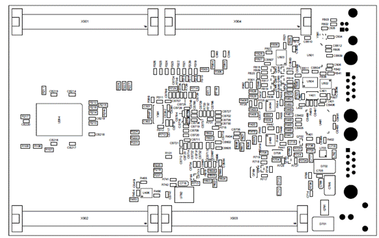
图15.TriBoard-TC179X V5.0评估板元件布局图(底层)
详情请见:
 TC1797_DS_V1 2.pdf (5.09 MB, 下载次数: 1) TC1797_DS_V1 2.pdf (5.09 MB, 下载次数: 1)
和
 TriBoardManual-TC179X-V50.pdf (3.08 MB, 下载次数: 7) TriBoardManual-TC179X-V50.pdf (3.08 MB, 下载次数: 7) |
|

