|
 
- UID
- 1023166
- 性别
- 男
- 来自
- 燕山大学
|

Renesas SH7269 266 MHz MCU开发方案
Renesas公司的SH7269是采用SH2A-FPU核的高性能MCU,片上SRAM为2.5MB,能直接显示WVGA(800x480象素)而不用外接SRAM,CPU工作频率266 MHz ,对设备控制和数字音频信号处理提高性能,主要用在汽车音频,HDD音频和网络音频,仪表盘和汽车显示系统以及机器人等.本文介绍了SH7269主要特性,方框图,以及SH7269 RSK评估板主要特性,方框图,电路图和评估板PCB元件布局图.
The SH7268, SH7269 Group are high-performance microcontrollers incorporating SH2A-FPU cores. The SH7268, SH7269 Group share the following features: (1) large-capacity 2.5 megabyte (MB) on-chip SRAM that is 1.7 times the capacity of the Renesas Electronics’ existing MCU (SH7266) allowing display of WVGA size (800 x 480 pixel) images without any external SRAM. (2) Increased maximum CPU operating frequency by approximately 1.8 times (266 MHz), which provides increased performance for device control and digital audio signal processing. (3) Additional functionalities, such as a 2D graphics accelerator that conforms to the OpenVG™ 1.1 standard, the industry standard graphics processing programming interface (API) for embedded equipment.
This LSI is a single-chip RISC (reduced instruction set computer) microcontroller that includes a Renesas-original RISC CPU as its core, and the peripheral functions required to configure a system.
The CPU in this LSI is an SH-2A CPU, which provides upward compatibility for SH-1, SH-2, and SH-2E CPUs at object code level. It has a RISC-type instruction set, superscalar architecture, and Harvard architecture, for superior rates of instruction execution. In addition, an independent 32-bit internal-bus architecture enhances data processing power. This CPU brings the user the ability to set up high-performance systems with strong functionality at less expense than was achievable with previous microcontrollers, and is even able to handle realtime control applications requiring high-speed characteristics.
This LSI has a floating-point unit and cache. In addition, this LSI includes on-chip peripheral functions necessary for system configuration, such as a 64-Kbyte RAM for high-speed operation, a 2.5-Mbyte large-capacity RAM (128-Kbytes are shared by the data-retention RAM), dataretention RAM, multi-function timer pulse unit 2, compare match timer, realtime clock, serial communication interface with FIFO, I2C bus interface 3, serial sound interface, clocked synchronous serial I/O with FIFO*2, controller area network*2, IEBusTM*1 controller, Renesas SPDIF interface, Renesas serial peripheral interface, Renesas quad serial peripheral interface, SPI multi I/O bus controller, CD-ROM decoder, A/D converter, NAND flash memory controller, USB 2.0 host/function, digital video decoder, video display controller 4, image renderer, display out comparison unit, OpenVG-compliant Renesas graphics processor, JPEG codec unit, sampling rate
converter, sound generator, SD host interface, MMC host interface, motor control PWM timer, interrupt controller modules, and general I/O ports.
This LSI also provides an external memory access support function to enable direct connection to various memory devices or peripheral LSIs. These on-chip functions significantly reduce costs of designing and manufacturing application systems.
SH7269主要特性:
Operating frequency
266 MHz
Cache
16 Kbytes (divided between instruction (8 KB) and data (8 KB), 4-way set associative)Debugging
H-UDI, AUD-Ⅱ
Packages
SH7268: 208-pin QFP(28mm x 28mm)(0.5mm pitch)
SH7269: 256-pin QFP(28mm x 28mm)(0.4mm pitch)
SH7269: 272-pin BGA(17mm x 17mm)(0.8mm pitch)
Other features
Large-capacity 2.5 MB on-chip SRAM supports one-chip solutions that do not require external SRAM
Achieves 266 MHz clock frequency high-speed operation
Improved display functions, including an OpenVG 1.1 conforming 2D graphics accelerator
SH7269主要应用:
[Audio] Car audio, HDD audio, and network audio, Graphical dashboard and vehicle display systems, [Industrial equipment] Sequencers, robots, etc.
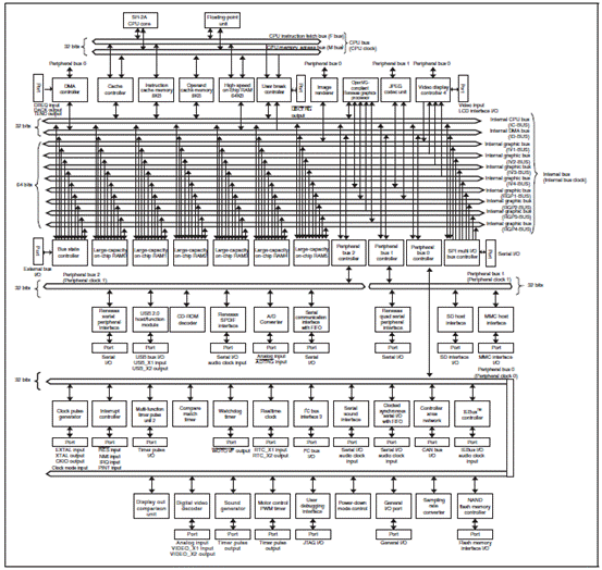
图1.SH7269方框图
SH7269 RSK评估板
Renesas Starter Kit2+ for SH7269
This RSK is an evaluation tool for Renesas microcontrollers. This manual describes the technical details of the RSK hardware. The Quick Start Guide and Tutorial Manual provide details of the software installation and debugging environment.
SH7269 RSK评估板主要特性:
This RSK provides an evaluation of the following features:
• Renesas microcontroller programming
• User code debugging
• User circuitry such as switches, LEDs and a potentiometer
• Sample application
• Sample peripheral device initialisation code
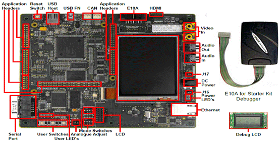
图2.SH7269 RSK评估板外形图
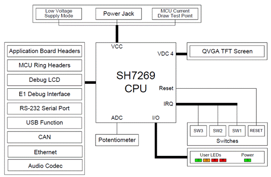
图3.SH7269 RSK评估板方框图
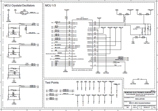
图4.SH7269 RSK评估板电路图(1)
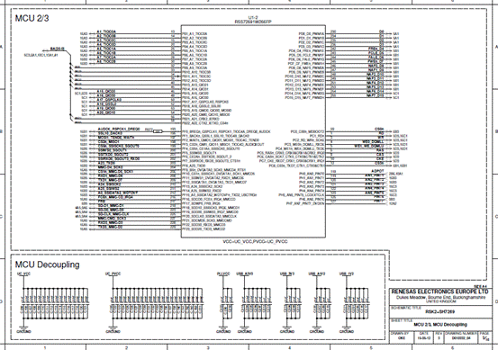
图5.SH7269 RSK评估板电路图(2)
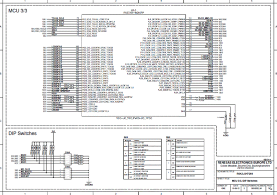
图6.SH7269 RSK评估板电路图(3)
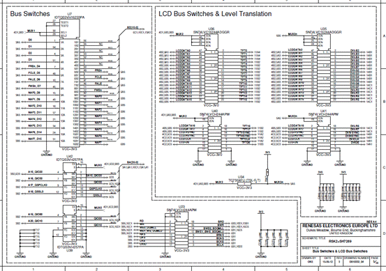
图7.SH7269 RSK评估板电路图(4)
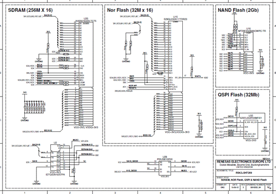
图8.SH7269 RSK评估板电路图(5)
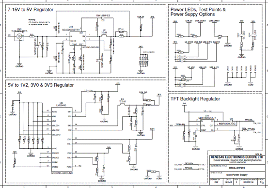
图9.SH7269 RSK评估板电路图(6)
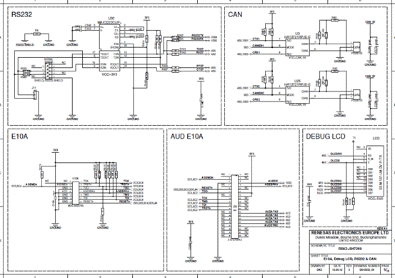
图10.SH7269 RSK评估板电路图(7)
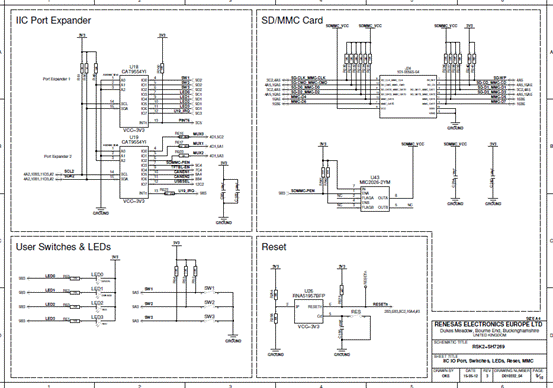
图11.SH7269 RSK评估板电路图(8)
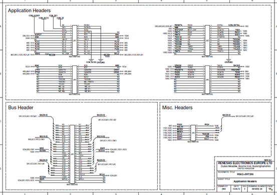
图12.SH7269 RSK评估板电路图(9)
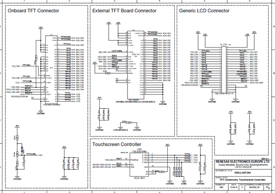
图13.SH7269 RSK评估板电路图(10)
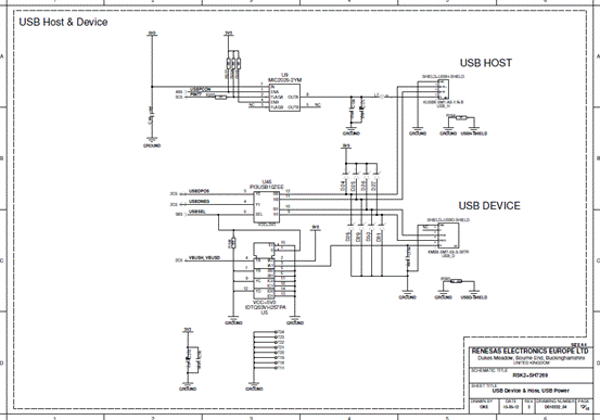
图14.SH7269 RSK评估板电路图(11)
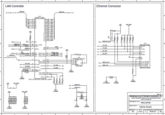
图15.SH7269 RSK评估板电路图(12)
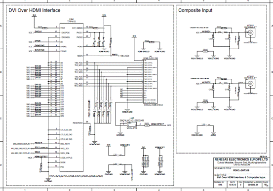
图16.SH7269 RSK评估板电路图(13)
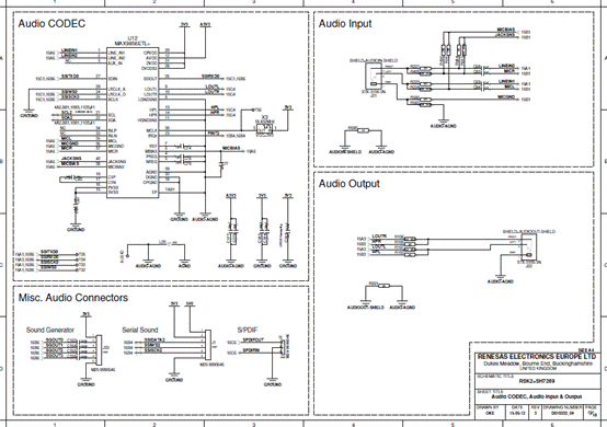
图17.SH7269 RSK评估板电路图(14)

图18.SH7269 RSK评估板电路图(15)
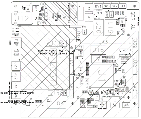
图19.SH7269 RSK评估板PCB元件布局图(顶层)
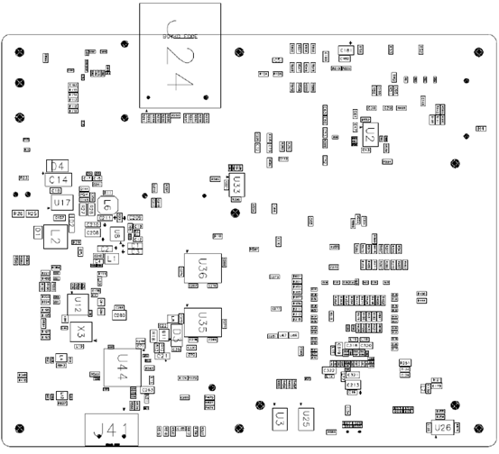
图20.SH7269 RSK评估板PCB元件布局图(底层)
详情请见:
 r20ut0591eg0300_rsk_plus_sh7269_schematics.pdf (348.21 KB, 下载次数: 1) r20ut0591eg0300_rsk_plus_sh7269_schematics.pdf (348.21 KB, 下载次数: 1)
和
 r20ut0592eg0100_rsk_plus_sh7269_usermanual.pdf (1.24 MB, 下载次数: 1) r20ut0592eg0100_rsk_plus_sh7269_usermanual.pdf (1.24 MB, 下载次数: 1)
以及
 r01uh0048ej_sh7268.pdf (17 MB, 下载次数: 1) r01uh0048ej_sh7268.pdf (17 MB, 下载次数: 1) |
|

