Microchip PIC18F46J50系列8位无线开发方案
|
 
- UID
- 1023166
- 性别
- 男
- 来自
- 燕山大学
|

Microchip PIC18F46J50系列8位无线开发方案
关键词: Microchip , PIC18F46J50
Microchip公司的PIC18F46J50系列是采用nanoWatt技术的8位MCU,具有高计算功能,丰富特性和极具价格竞争能力.因此具有广泛应用,特别是那些首要考虑成本的地方.本文介绍了PIC18F46J50系列主要特性和方框图,以及8位无线开发套件(用于近1GHz和2.4GHz RF)主要特性,电路图,材料清单和元件布局图.
This PIC18F46J50 family introduces a new line of low-voltage Universal Serial Bus (USB) microcontrollers with the main traditional advantage of all PIC18 microcontrollers, namely, high computational performance and a rich feature set at an extremely competitive price point. These features make the PIC18F46J50 family a logical choice for many high-performance applications, where cost is a primary consideration.
PIC18FxxJxx系列主要特性:
1. nanoWatt TECHNOLOGY
All of the devices in the PIC18F46J50 family incorporate a range of features that can significantly reduce power consumption during operation. Key features are:
• Alternate Run Modes: By clocking the controller from the Timer1 source or the internal RC oscillator, power consumption during code execution can be reduced by as much as 90%.
• Multiple Idle Modes: The controller can also run with its CPU core disabled but the peripherals still active. In these states, power consumption can be reduced even further, to as little as 4% of normal operational requirements.
• On-the-Fly Mode Switching: The power-managed modes are invoked by user code during operation, allowing the users to incorporate power-saving ideas into their application’s software design.
2. UNIVERSAL SERIAL BUS (USB)
Devices in the PIC18F46J50 family incorporate a fully-featured USB communications module with a built-in transceiver that is compliant with the “USB Specification Revision 2.0”. The module supports both low-speed and full-speed communication for all supported data transfer types.
3. OSCILLATOR OPTIONS AND FEATURES
All of the devices in the PIC18F46J50 family offer five different oscillator options, allowing users a range of choices in developing application hardware. These include:
• Two Crystal modes, using crystals or ceramic resonators.
• Two External Clock modes, offering the option of a divide-by-4 clock output.
• An internal oscillator block, which provides an 8 MHz clock and an INTRC source (approximately 31 kHz, stable over temperature and VDD), as well as a range of six user-selectable clock frequencies, between 125 kHz to 4 MHz, for a total of eight clock frequencies. This option frees an oscillator pin for use as an additional general purpose I/O.
• A Phase Lock Loop (PLL) frequency multiplier, available to the high-speed crystal, and external and internal oscillators, providing a clock speed up to 48 MHz.
• Dual clock operation, allowing the USB module to run from a high-frequency oscillator while the rest of the microcontroller is clocked at a different frequency.
The internal oscillator block provides a stable reference source that gives the PIC18F46J50 family additional features for robust operation:
• Fail-Safe Clock Monitor: This option constantly monitors the main clock source against a reference signal provided by the internal oscillator. If a clock failure occurs, the controller is switched to the internal oscillator, allowing for continued low-speed operation or a safe application shutdown.
• Two-Speed Start-up: This option allows the internal oscillator to serve as the clock source from Power-on Reset (POR), or wake-up from Sleep mode, until the primary clock source is available.
4. EXPANDED MEMORY
The PIC18F46J50 family provides ample room for application code, from 16 Kbytes to 64 Kbytes of code space. The Flash cells for program memory are rated to last in excess of 10000 erase/write cycles. Data retention without refresh is conservatively estimated to be greater than 20 years.
The Flash program memory is readable and writable during normal operation. The PIC18F46J50 family also provides plenty of room for dynamic application data with up to 3.8 Kbytes of data RAM.
5. EXTENDED INSTRUCTION SET
The PIC18F46J50 family implements the optional extension to the PIC18 instruction set, adding eight new instructions and an Indexed Addressing mode.
Enabled as a device configuration option, the extension has been specifically designed to optimize re-entrant application code originally developed in high-level languages, such as C.
6. EASY MIGRATION
Regardless of the memory size, all devices share the same rich set of peripherals, allowing for a smooth migration path as applications grow and evolve.
The consistent pinout scheme used throughout the entire family also aids in migrating to the next larger device.
The PIC18F46J50 family is also pin compatible with other PIC18 families, such as the PIC18F4550, PIC18F2450 and PIC18F45J10. This allows a new dimension to the evolution of applications, allowing developers to select different price points within Microchip’s PIC18 portfolio, while maintaining the same feature set.
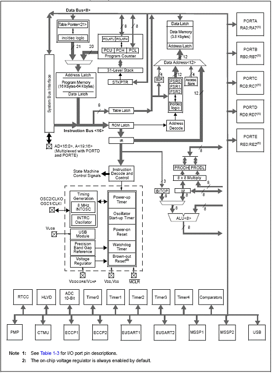
图1.PIC18F4XJ50 (44引脚)方框图
8位无线开发套件
The Wireless Development Kit allows developers to evaluate and experiment with sub-GHz and 2.4 GHz RF solutions from Microchip. The Wireless Development Kit provides two RF hardware nodes which can be used to create a simple two-node wireless network. More nodes can be added by purchasing 8-Bit Wireless Development Kit or individual components.
The 8-Bit Wireless Development Kit is pre-programmed with a wireless demo program that allows multiple operational configurations to be tested without writing any firmware. For more information on how to operate the pre-programmed demo program and how to develop other applications. It also enables customer to evaluate Microchip’s proprietary wireless stacks. The Microchip wireless stacks and additional application demo source codes can be downloaded from the Microchip web sitehttp://www.microchip.com/wireless.
The PIC18 Wireless Development Board provides all the necessary components required to build an extreme low power wireless sensor application. The Serial Accessory Port can interface external sensors or modules, like LCD Serial Accessory Board or RS232 Serial Accessory Board. The platform provides USB connectivity and supports different XLP microcontroller options.
The PIC18 Wireless Development Board supports the XLP microcontroller options such as PIC18F46J11, PIC18F46J50, PIC18F46K20 and PIC18LF45K22.
The default microcontroller option is PIC18F46J50. Different microcontroller options require different components to populate on the board.
The following main blocks are defined on the Board:
•Serial Accessory Port
•USB Interface Port
• ICtail Port ICtail Port
• ush Buttons ush Buttons
•Onboard Temperature Sensor
•Onboard Serial EEPROM
•Debug LEDs
• ower Supply ower Supply
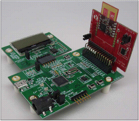
图2. PIC18无线开发套件外形图
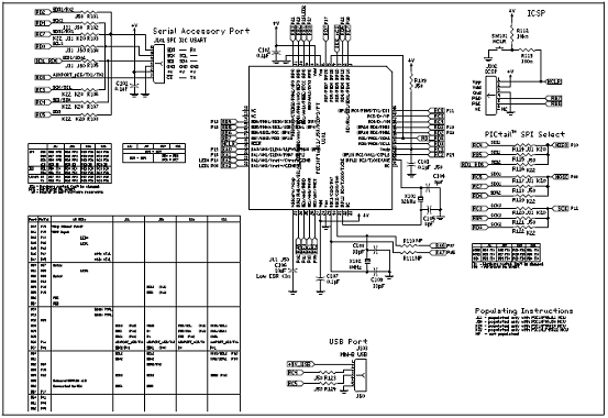
图3. PIC18无线开发套件电路图(1)
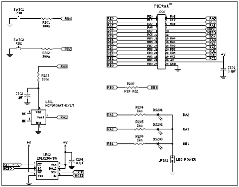
图4. PIC18无线开发套件电路图(2)
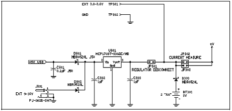
图5.PIC18无线开发套件电路图(3)
PIC18无线开发套件材料清单:
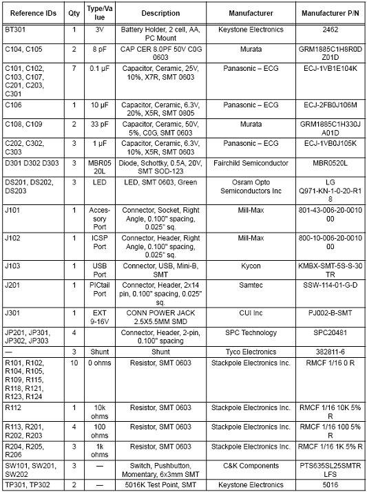
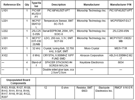
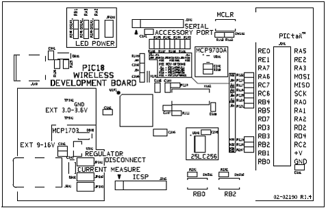
图8.PIC18无线开发套件元件布局图
详情请见:
http://ww1.microchip.com/downloads/en/DeviceDoc/39931d.pdf
和
http://ww1.microchip.com/downloads/en/DeviceDoc/70654A.pdf |
|
|
|
|
|
|

