|

- UID
- 1023166
- 性别
- 男
- 来自
- 燕山大学
|

ST EVALSP1340CPU嵌入600MHz MPU开发方案
关键词: CPU , EVALSP1340 , MPU , ST
ST公司的SPEAr1340是SPEAr®(结构处理器增强架构)系列微处理器的系统级芯片(SoC),CPU子系统采用高达600MHz的2x ARM Cortex A9核,每个核有32+32 KB L1高速缓存,共享的512KB L2高速缓存,高达166MHz的片上网络总线矩阵, 32KB引导ROM,32+4KB静态RAM,主要用于低成本平板电脑,薄型客户端,媒体手机和工业/打印机智能屏.本文介绍了SPEAr1340主要特性,架构框图以及EVALSP1340CPU评估板主要特性,框图,电路图,材料清单和PCB布局图.
The SPEAr1340 device is a system-on-chip belonging to the SPEAr® (Structured Processor Enhanced Architecture) family of embedded microprocessors. The product is suitable for consumer and professional applications where an advanced human machine interface (HMI) combined with high performance are required, such as low-cost tablets, thin clients, media phones and industrial/printer smart panels.
The device is hardware-compliant to the support of both real-time (RTOS) and high-level (HLOS) operating systems, such as Android, Linux and Windows Embedded Compact 7.
The architecture of SPEAr1340 is based on several internal components, communicating through a multilayer interconnection matrix (BUSMATRIX). This switching structure enables different data flows to be carried out concurrently, improving the overall platform efficiency.
In particular, high-performance master agents are directly interconnected with the DDR memory controller in order to reduce access latency. The overall memory bandwidth assigned to each master port can be programmed and optimized through an internal weighted round-robin (WRR) arbitration scheme.
SPEAr1340主要特性:
■ CPU subsystem:
– 2x ARM Cortex A9 cores, up to 600 MHz
– 32+32 KB L1 caches per core, with parity check
– Shared 512 KB L2 cache
– Accelerator coherence port (ACP)
■ Network-on-chip bus matrix, up to 166 MHz
■ 32 KB Boot ROM, 32+4 KB Static RAMs
■ Memory interfaces:
– DDR controller (DDR3-1066, DDR2-800), 16-/32-bit, up to 2 GB address space
– Serial NOR Flash controller
– Parallel NAND Flash/NOR Flash/SRAM controller
■ Connectivity:
– 2 x USB 2.0 Host ports (integrated PHY)
– 1 x USB 2.0 OTG port (integrated PHY)
– 1 x Giga/Fast Ethernet port (external GMII/ RGMII/MII/RMII PHY)
– 1 x PCIe 2.0 RC/EP port (integrated PHY)
– 1 x 3Gb/s Serial ATA Host port (integrated PHY)
– 1 x memory card interface: SDIO/MMC, CF/CF+, xD
– 2 x UART ports, with IrDA option
– 2 x I2C bus controllers, master/slave
– 1 x synchronous serial port, SPI/Microwire/TI protocols, master/slave
– 2 x consumer electronic control (HDMI CEC) ports
– 10-bit ADC: 8 channels, 1 Msps, with autoscan
– Programmable bidirectional GPIO signals with interrupt capability
■ HMI support:
– LCD display controller, up to 1920 x 1200, 60 Hz, 24 bpp
High-performance 2D/3D GPU, up to 1080p
– Hardware video decoder: multistandard up to 1080p, JPEG
– Hardware video encoder: H.264 up to 1080p, JPEG
– Video input parallel port, with alternate configuration for 4 x camera interfaces – Digital audio ports: up to 7.1 multichannel surround, I2S (8 in, 8 out) and S/PDIF – 6 x 6 keyboard controller
– Resistive touchscreen interface
■ Security:
– Cryptographic co-processor: DES, 3DES, AES, HMAC, PKA, RNG
■ Miscellaneous functions:
– Energy saving: power islands, clock gating, dynamic frequency scaling
– 2 x DMA controllers (total 16 channels)
– 11 x general purpose timers, 2 x watchdogs, 1 x real-time clock
– 4 x PWM generators
– Embedded sensor for junction temperature monitoring
OTP (one-time programmable) bits
– Debug and trace interfaces: JTAG/PTM
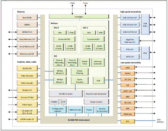
图1.SPEAr1340架构框图
EVALSP1340CPU评估板
This evaluation board is intended to be used to:
● enable quick evaluate and debugging of software for the SPEAr1340 embedded MPU
● act as a learning tool for rapid familiarity with the features of the SPEAr1340
● provide a reference design to use as a starting point for the development of a final application board
The EVALSP1340CPU board is equipped with interfaces to the high-speed peripherals embedded in SPEAr1340 device.
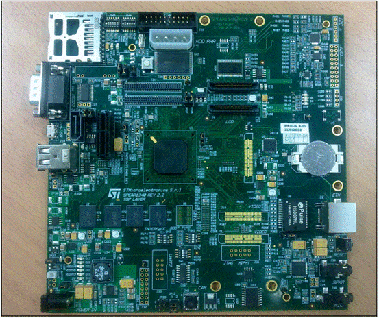
图2.EVALSP1340CPU评估板外形图
EVALSP1340CPU评估板主要特性:
● SPEAr1340 embedded MPU
● 4 DDR3 chips (32-bit) 1 GB
● Serial NOR Flash, 8 MB
● 8-bit NAND Flash, 2 Gb
● 16-bit NAND Flash expansion connector
● Audio stereo jack and microphone
● Two USB 2.0 high speed host ports
● One OTG 2.0 high speed port (Micro USB-AB)
● One 10/100/1000 Ethernet port
● One PCIe X1 Root Complex connector
● One SATA connector
● One SDIO connector
● One UART serial port (up to 115 Kbaud)
● LCD connectors (LVDS bus - TFT panel)
● Camera module
● MEMS (accelerometer & magnetometer)
● Debug port (CPU JTAG connector)
Optional
● 10" LCD kit - order code EVALSP1340LCD
● CLCD Video HDMI transmitter plugboard - order code EVALSP1340HDM
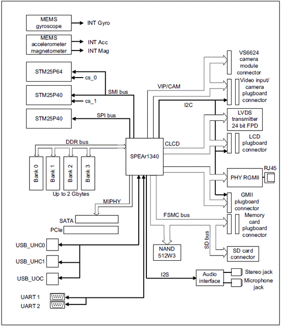
图3.EVALSP1340CPU评估板方框图

图4.EVALSP1340CPU评估板电路图(1)
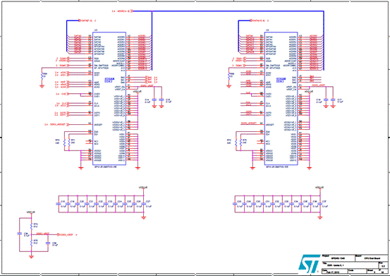
图5.EVALSP1340CPU评估板电路图(2)
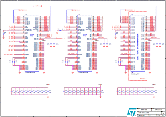
图6.EVALSP1340CPU评估板电路图(3)
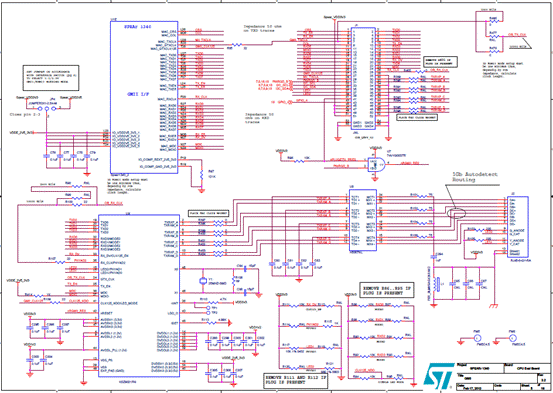
图7.EVALSP1340CPU评估板电路图(4)

图8.EVALSP1340CPU评估板电路图(5)
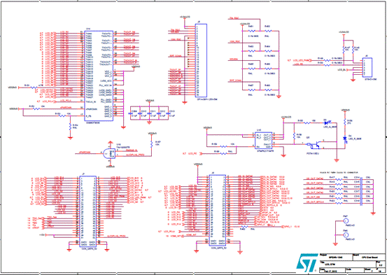
图9.EVALSP1340CPU评估板电路图(6)

图10.EVALSP1340CPU评估板电路图(7)

图11.EVALSP1340CPU评估板电路图(8)

图12.EVALSP1340CPU评估板电路图(9)
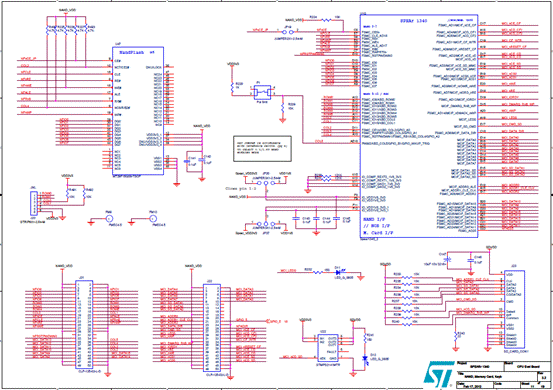
图13.EVALSP1340CPU评估板电路图(10)
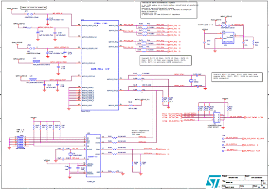
图14.EVALSP1340CPU评估板电路图(11)
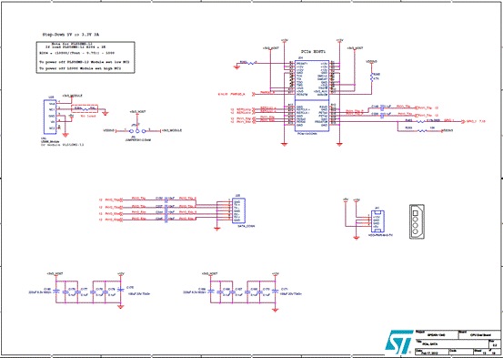
图15.EVALSP1340CPU评估板电路图(12)
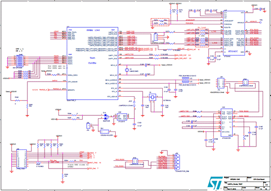
图16.EVALSP1340CPU评估板电路图(13)
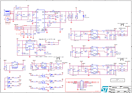
图17.EVALSP1340CPU评估板电路图(14)

图18.EVALSP1340CPU评估板电路图(15)

图19.EVALSP1340CPU评估板电路图(16)

图20.EVALSP1340CPU评估板电路图(17)
EVALSP1340CPU评估板材料清单:
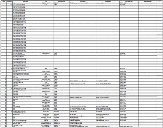
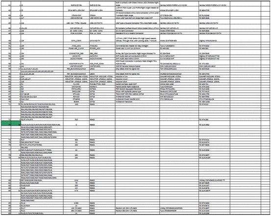  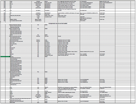 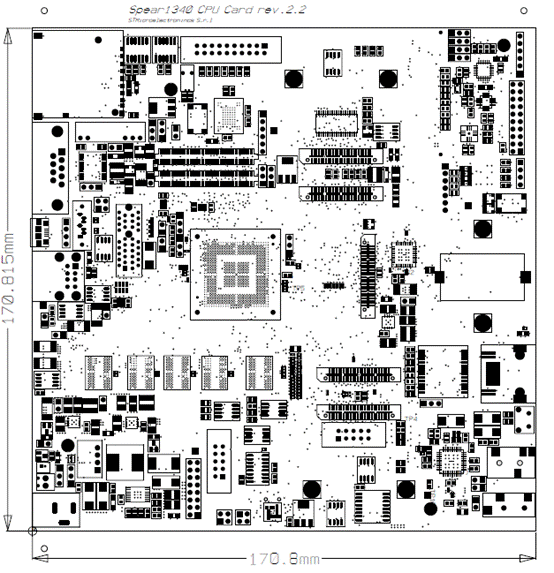 图21.EVALSP1340CPU评估板元件布局图(1) 图21.EVALSP1340CPU评估板元件布局图(1)

图22.EVALSP1340CPU评估板元件布局图(2)

图23.EVALSP1340CPU评估板元件布局图(3)
详情请见:
 DM00049696.pdf (1.47 MB, 下载次数: 17) DM00049696.pdf (1.47 MB, 下载次数: 17)
和
DM00052367.pdf (2.06 MB, 下载次数: 15)
以及
evalsp1340cpu_schematics.pdf (511.91 KB, 下载次数: 12) |
|
|


