|
 
- UID
- 1023166
- 性别
- 男
- 来自
- 燕山大学
|

Embest Luminary LM3S8962 Cortex-M3 32位MCU开发评估方案
Embest公司的EKK8962 ARM评估板是基于Luminary公司的Stellaris LM3S8962 (ARM Cortex-M3核) 32位MCU,是简单和通用的评估平台,具有多种硬件源如10/100 MB以太网接口,CAN,128×96 OLED
LCD,扬声器,MicroSD卡插座,USB和标准20引脚JTAG接口.可应用于遥控,POS机,测试测量,网络设备,工厂自动化,HVAC和建筑物控制,马达驱动,医疗设备,能源和交通等.本文介绍了LM3S8962主要特性,方框图和CPU方框图以及Embest EKK8962 ARM评估板主要特性,方框图,电路图和元件布局图.
The Luminary Micro Stellaris?family of microcontrollers he first ARM?Cortex?M3 based Controllers rings high-performance 32-bit computing to cost-sensitive embedded microcontroller applications. These pioneering parts deliver customers 32-bit performance at a cost equivalent to legacy 8- and 16-bit devices, all in a package with a small footprint.
The Stellaris?family offers efficient performance and extensive integration, favorably positioning the device into cost-conscious applications requiring significant control-processing and connectivity capabilities. The Stellaris?LM3S2000 series, designed for Controller Area Network (CAN) applications, extends the Stellaris family with Bosch CAN networking technology, the golden standard in short-haul industrial networks. The Stellaris?LM3S2000 series also marks the first integration of CAN capabilities with the revolutionary Cortex-M3 core. The Stellaris?LM3S6000 series combines both a 10/100 Ethernet Media Access Control (MAC) and Physical (PHY) layer, marking the first time that integrated connectivity is available with an ARM Cortex-M3 MCU and the only integrated 10/100 Ethernet MAC and PHY available in an ARM architecture MCU.
The LM3S8962 microcontroller is targeted for industrial applications, including remote monitoring, electronic point-of-sale machines, test and measurement equipment, network appliances and switches, factory automation, HVAC and building control, gaming equipment, motion control, medical instrumentation, and fire and security.
For applications requiring extreme conservation of power, the LM3S8962 microcontroller features a Battery-backed Hibernation module to efficiently power down the LM3S8962 to a low-power state during extended periods of inactivity. With a power-up/power-down sequencer, a continuous time counter (RTC), a pair of match registers, an APB interface to the system bus, and dedicated non-volatile memory, the Hibernation module positions the LM3S8962 microcontroller perfectly for battery applications.
In addition, the LM3S8962 microcontroller offers the advantages of ARM’s widely available development tools, System-on-Chip (SoC) infrastructure IP applications, and a large user community.
Additionally, the microcontroller uses ARM’s Thumb?compatible Thumb-2 instruction set to reduce memory requirements and, thereby, cost. Finally, the LM3S8962 microcontroller is code-compatible to all members of the extensive Stellaris?family; providing flexibility to fit our customers’ precise needs.
Luminary Micro offers a complete solution to get to market quickly, with evaluation and development boards, white papers and application notes, an easy-to-use peripheral driver library, and a strong support, sales, and distributor network.
LM3S8962主要特性:
The LM3S8962 microcontroller includes the following product features:
■ 32-Bit RISC Performance
– 32-bit ARM® Cortex™-M3 v7M architecture optimized for small-footprint embedded applications
–System timer (SysTick), providing a simple, 24-bit clear-on-write, decrementing, wrap-on-zero counter with a flexible control mechanism
–Thumb®-compatible Thumb-2-only instruction set processor core for high code density
–50-MHz operation
– Hardware-division and single-cycle-multiplication
– Integrated Nested Vectored Interrupt Controller (NVIC) providing deterministic interrupt handling
– 36 interrupts with eight priority levels
– Memory protection unit (MPU), providing a privileged mode for protected operating system functionality
– Unaligned data access, enabling data to be efficiently packed into memory
– Atomic bit manipulation (bit-banding), delivering maximum memory utilization and streamlined peripheral control
■ Internal Memory
– 256 KB single-cycle flash
• User-managed flash block protection on a 2-KB block basis
• User-managed flash data programming
• User-defined and managed flash-protection block
– 64 KB single-cycle SRAM
■ General-Purpose Timers
– Four General-Purpose Timer Modules (GPTM), each of which provides two 16-bit timer/counters. Each GPTM can be configured to operate independently as timers or event counters: as a single 32-bit timer, as one 32-bit Real-Time Clock (RTC) to event capture, for Pulse Width Modulation (PWM), or to trigger analog-to-digital conversions
– 32-bit Timer modes
• Programmable one-shot timer
• Programmable periodic timer
• Real-Time Clock when using an external 32.768-KHz clock as the input
• User-enabled stalling in periodic and one-shot mode when the controller asserts the CPU Halt flag during debug
• ADC event trigger
– 16-bit Timer modes
• General-purpose timer function with an 8-bit prescaler
• Programmable one-shot timer
• Programmable periodic timer
• User-enabled stalling when the controller asserts CPU Halt flag during debug
• ADC event trigger
– 16-bit Input Capture modes
• Input edge count capture
• Input edge time capture
– 16-bit PWM mode
• Simple PWM mode with software-programmable output inversion of the PWM signal
■ ARM FiRM-compliant Watchdog Timer
– 32-bit down counter with a programmable load register
– Separate watchdog clock with an enable
– Programmable interrupt generation logic with interrupt masking
– Lock register protection from runaway software
– Reset generation logic with an enable/disable
– User-enabled stalling when the controller asserts the CPU Halt flag during debug
■ Controller Area Network (CAN)
– Supports CAN protocol version 2.0 part A/B
– Bit rates up to 1Mb/s
– 32 message objects, each with its own identifier mask
– Maskable interrupt
– Disable automatic retransmission mode for TTCAN
– Programmable loop-back mode for self-test operation
■ 10/100 Ethernet Controller
– Conforms to the IEEE 802.3-2002 Specification
– IEEE 1588-2002 Precision Time Protocol (PTP) compliant
– Full- and half-duplex for both 100 Mbps and 10 Mbps operation
– Integrated 10/100 Mbps Transceiver (PHY)
– Automatic MDI/MDI-X cross-over correction
– Programmable MAC address
– Power-saving and power-down modes
■ Synchronous Serial Interface (SSI)
– Master or slave operation
– Programmable clock bit rate and prescale
– Separate transmit and receive FIFOs, 16 bits wide, 8 locations deep
– Programmable interface operation for Freescale SPI, MICROWIRE, or Texas Instruments synchronous serial interfaces
– Programmable data frame size from 4 to 16 bits
– Internal loopback test mode for diagnostic/debug testing
■ UART
– Two fully programmable 16C550-type UARTs with IrDA support
– Separate 16x8 transmit (TX) and 16x12 receive (RX) FIFOs to reduce CPU interrupt service loading
– Programmable baud-rate generator with fractional divider
– Programmable FIFO length, including 1-byte deep operation providing conventional double-buffered interface
– FIFO trigger levels of 1/8, 1/4, 1/2, 3/4, and 7/8
– Standard asynchronous communication bits for start, stop, and parity
– False-start-bit detection
– Line-break generation and detection
■ ADC
– Single- and differential-input configurations
– Four 10-bit channels (inputs) when used as single-ended inputs
– Sample rate of 500 thousand samples/second
– Flexible, configurable analog-to-digital conversion
– Four programmable sample conversion sequences from one to eight entries long, with corresponding conversion result FIFOs
– Each sequence triggered by software or internal event (timers, analog comparators, PWM or GPIO)
– On-chip temperature sensor
■ Analog Comparators
– One integrated analog comparator
– Configurable for output to: drive an output pin, generate an interrupt, or initiate an ADC sample sequence
– Compare external pin input to external pin input or to internal programmable voltage reference
■ I2C
– Master and slave receive and transmit operation with transmission speed up to 100 Kbps in Standard mode and 400 Kbps in Fast mode
– Interrupt generation
– Master with arbitration and clock synchronization, multimaster support, and 7-bit addressing mode
■ PWM
– Three PWM generator blocks, each with one 16-bit counter, two comparators, a PWM generator, and a dead-band generator
– One 16-bit counter
• Runs in Down or Up/Down mode
• Output frequency controlled by a 16-bit load value
• Load value updates can be synchronized
• Produces output signals at zero and load value
– Two PWM comparators
• Comparator value updates can be synchronized
• Produces output signals on match
– PWM generator
• Output PWM signal is constructed based on actions taken as a result of the counter and PWM comparator output signals
• Produces two independent PWM signals
– Dead-band generator
• Produces two PWM signals with programmable dead-band delays suitable for driving a half-H bridge
• Can be bypassed, leaving input PWM signals unmodified
– Flexible output control block with PWM output enable of each PWM signal
• PWM output enable of each PWM signal
• Optional output inversion of each PWM signal (polarity control)
• Optional fault handling for each PWM signal
• Synchronization of timers in the PWM generator blocks
• Synchronization of timer/comparator updates across the PWM generator blocks
• Interrupt status summary of the PWM generator blocks
– Can initiate an ADC sample sequence
■ QEI
– Two QEI modules
– Hardware position integrator tracks the encoder position
– Velocity capture using built-in timer
– Interrupt generation on index pulse, velocity-timer expiration, direction change, and quadrature error detection
■ GPIOs
– 5-42 GPIOs, depending on configuration
– 5-V-tolerant input/outputs
– Programmable interrupt generation as either edge-triggered or level-sensitive
– Bit masking in both read and write operations through address lines
– Can initiate an ADC sample sequence
– Programmable control for GPIO pad configuration:
• Weak pull-up or pull-down resistors
• 2-mA, 4-mA, and 8-mA pad drive
• Slew rate control for the 8-mA drive
• Open drain enables
• Digital input enables
■ Power
– On-chip Low Drop-Out (LDO) voltage regulator, with programmable output user-adjustable from 2.25 V to 2.75 V
– Hibernation module handles the power-up/down 3.3 V sequencing and control for the core digital logic and analog circuits
– Low-power options on controller: Sleep and Deep-sleep modes
– Low-power options for peripherals: software controls shutdown of individual peripherals
– User-enabled LDO unregulated voltage detection and automatic reset
– 3.3-V supply brown-out detection and reporting via interrupt or reset
■ Flexible Reset Sources
– Power-on reset (POR)
– Reset pin assertion
– Brown-out (BOR) detector alerts to system power drops
– Software reset
– Watchdog timer reset
– Internal low drop-out (LDO) regulator output goes unregulated
■ Additional Features
– Six reset sources
– Programmable clock source control
– Clock gating to individual peripherals for power savings
– IEEE 1149.1-1990 compliant Test Access Port (TAP) controller
– Debug access via JTAG and Serial Wire interfaces
– Full JTAG boundary scan
■ Industrial-range 100-pin RoHS-compliant LQFP package
LM3S8962目标应用:
■ Remote monitoring
■ Electronic point-of-sale (POS) machines
■ Test and measurement equipment
■ Network appliances and switches
■ Factory automation
■ HVAC and building control
■ Gaming equipment
■ Motion control
■ Medical instrumentation
■ Fire and security
■ Power and energy
■ Transportation

图1.Stellaris LM3S8962方框图
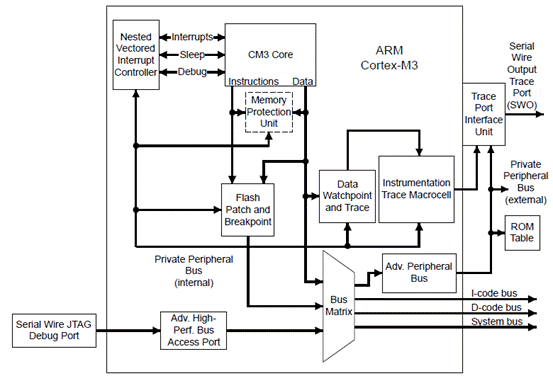
图2.Stellaris LM3S8962 CPU方框图
Embest EKK8962 ARM评估板
EKK8962 arm evaluation board produced by Embest is a Stellaris LM3S8962(ARM®Cortex -M3 core)microcontroller based simple and general purpose evaluation platform. This platform features various hardware resources: 10/100 MB Ethernet interface, CAN, 128×96 OLED LCD, speaker, MicroSD card socket, USB, standard 20-pin JTAG interface. The outstanding feature of this board is that the board integrates debugger, you just need an USB cable, then you can easily implement debug and download flash with the MDK software in your host pc.
Embest EKK8962 ARM评估板主要特性:
The Stellaris LM3S8962 Evaluation Kit includes the following features:
􀂄 Stellaris LM3S8962 microcontroller with fully-integrated 10/100 embedded Ethernet controller and CAN module
􀂄 Simple setup; USB cable provides serial communication, debugging, and power
􀂄 OLED graphics display with 128 x 96 pixel resolution
􀂄 User LED, navigation switches, and select pushbuttons
􀂄 Magnetic speaker
􀂄 MicroSD card slot
􀂄 USB interface for debugging and power supply
􀂄 Standard ARM® 20-pin JTAG debug connector with input and output modes
􀂄 LM3S8962 I/O available on labeled break-out pads
􀂄 Standalone CAN device board using Stellaris LM3S2110 microcontroller
The evaluation kit contains everything needed to develop and run applications for Stellaris microcontrollers including:
􀂄 LM3S8962 evaluation board (EVB)
􀂄 LM3S2110 CAN device board
􀂄 USB cable
􀂄 20-pin JTAG/SWD target cable
􀂄 10-pin CAN cable
􀂄 CD containing:
– A supported version of one of the following:
• Keil™ RealView® Microcontroller Development Kit (MDK-ARM)
• IAR Embedded Workbench
• Code Sourcery GCC development tools
– Complete documentation
– Quickstart guide
Quickstart source code
– DriverLib and example source code

图3.Embest EKK8962以太网和CAN评估板外形图

图4. Stellaris LM3S8962 评估板元件布局图
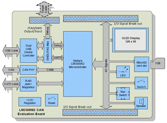
图5. Stellaris LM3S8962 评估板方框图
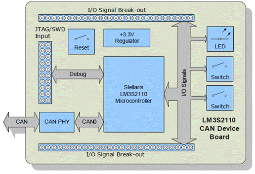
图6.LM3S2110 CAN器件方框图

图7. Stellaris LM3S8962 评估板电路图(1)
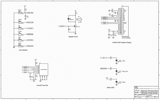
图8. Stellaris LM3S8962 评估板电路图(2)
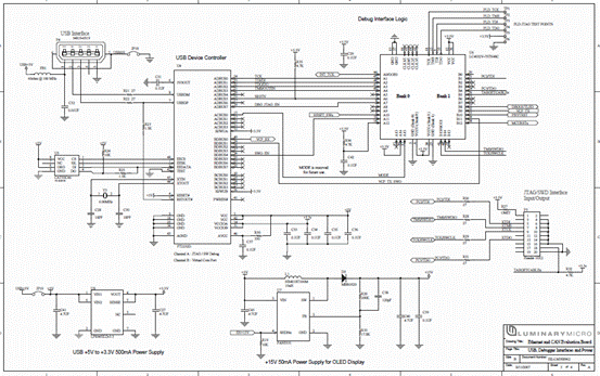
图9. Stellaris LM3S8962 评估板电路图(3)
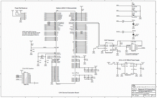
图10. Stellaris LM3S8962 评估板电路图(4)
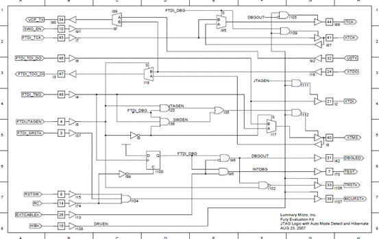
图11. Stellaris LM3S8962 评估板电路图(5)
详情请见:
 EK-LM3S8962_EvalBoard_UserManual[1].pdf (1.34 MB, 下载次数: 2) 和 EK-LM3S8962_EvalBoard_UserManual[1].pdf (1.34 MB, 下载次数: 2) 和
 Datasheet_LM3S8962[1].pdf (5.93 MB, 下载次数: 0) Datasheet_LM3S8962[1].pdf (5.93 MB, 下载次数: 0) |
|

