|

- UID
- 1029342
- 性别
- 男
|

(1)DBI接口
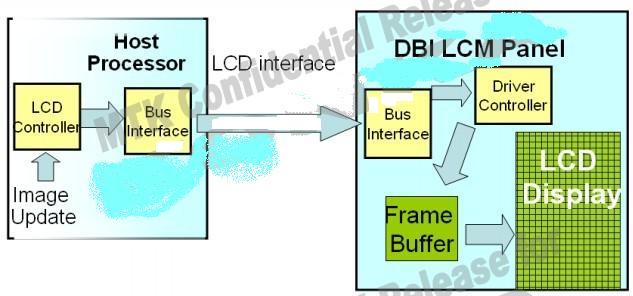
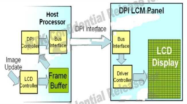
A,也就是通常所讲的MCU借口,俗称80 system接口。The lcd interface between host processor and LCM device list as below,The LCM driver will repeated update panel display。MCU借口通过并行接口传输控制命令和数据,并通过往LCM模组自带的GRAM(graphic RAM)更新数据实现屏幕的刷新。
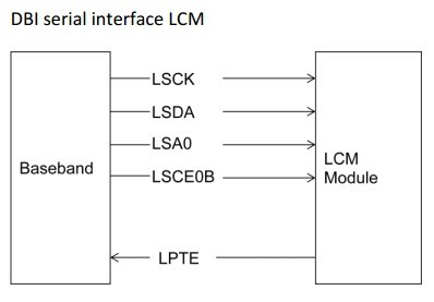
DBI接口分为串行和并行两种,模型如下:
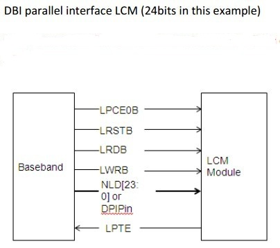 
B,以典型的18位数据跟16位数据做说明(8位寄存器控制)。
如上硬件采用18位数据线,控制命令和参数占用DB0到DB7并行传输,图像数据采用RGB666的格式并行传输。
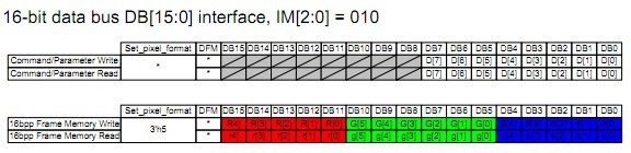
如上硬件采用16位数据线,控制命令和参数占用DB0到DB7并行传输,图像数据采用RGB565的格式并行传输。
C,关于DBI data format的说明
(I)对于16位的datawidth,典型的数据格式举例如下
1cycle/1pixel,RGB565,格式是:rrrrrggggggbbbbb
3cycle/2pixel,RGB666,格式是:xxxxrrrrrrgggggg
xxxxbbbbbbrrrrrr
xxxxggggggbbbbbb
3cycle/2pixel,RGB888,格式是:rrrrrrrrgggggggg
bbbbbbbbrrrrrrrr
ggggggggbbbbbbbb
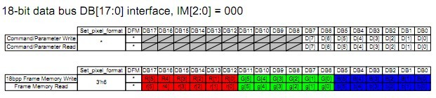
(II)对于18位的datawidth,典型的数据格式举例如下
1cycle/1pixel,RGB666,格式是:rrrrrrggggggbbbbbb
3cycle/2pixel,RGB888,格式是:rrrrrrrrgggggggg
bbbbbbbbrrrrrrrr
ggggggggbbbbbbbb
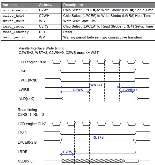
D,硬件接口及时序
(I)硬件连接图:
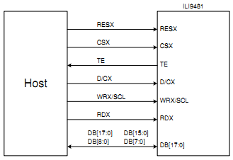
RESX:复位;CSX:chip select片选;TE:tearing enable;D/CX:register select寄存器选择;WRX/SCL:write control;RDX:read control;DB[....]:传输线。
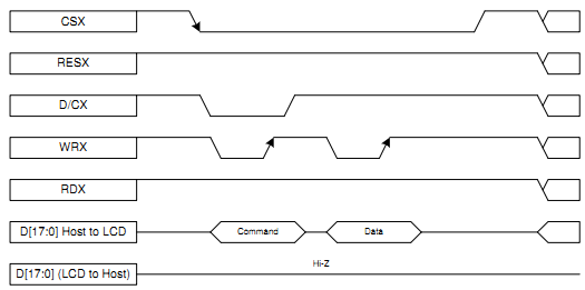
(II)写周期:
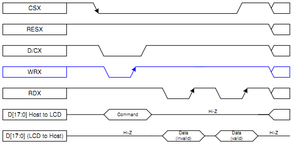
(III)读周期:
(IV)关于屏参中6个读写时序
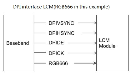
(2)DPI接口
也就是通常所说的RGB接口,采用普通的同步、时钟、信号线来传输特定数据,采用SPI等控制线完成命令控制。某种程度上,DPI与DBI的最大差别是,DPI的数据线和控制线分离,而DBI是复用的。
它的模型如下:
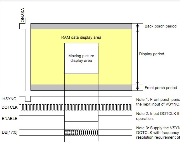
它的信号时序图如下:
曾经在调试一个DPI接口LCM时碰到一个奇怪现象,RGB的接口用一个LVDS转换芯片跟一款LVDS模组相连。重烧程序完后可以显示图像,断电再上电就没有图像,后来发现是上电屏参初始化中没有配置一个CS拉高的使能信号脚。烧完程序后改脚为高所以可以显示,重断电再上电默认为低所以没有图像。
(3)DPI与DBI的兼容
现在很多LCM的模组可以做到DBI和DPI接口的兼容。因为在IM2/IM1/IM0由手机主板决定的前提下,比如6516支持MCU接口,同时该模组放到另一款DPI接口的主板上也可以照样使用。
另一个补充问题,关于显示位数,由于嵌入式WINDOWS系统的GUI是16位的,不同于桌面WINDOWS的32位,所以24位的位图在WIN CE中,只能以16位色显示,一定会丢掉某些颜色。这个缺陷还在于,就算是18(RGB666)位的LCM数据位显式,最终软件中接受的GUI颜色还是16位,要把RGB565转成RGB666才能当18位色显示,相当于插值了。 |
|


 好帖好帖,路过帮顶