|
 
- UID
- 852722
|

Renesas公司的RX62T是100MHz 32位RX CPU内核的MCU,在100MHz时具有165DMIPS性能,单精度32位IEEE-754浮点,累加器能从32x32位运算中处理64位结果,乘法和除法能处理32x32运算,具有快速中断功能,CPU工作电压3.3V或5V,主要用在马达控制,通用逆变器等.本文介绍了RX62T主要特性,方框图,RX62T RSK评估板主要特性,方框图,电路图和PCB元件布局图.
100-MHz 32-bit RX MCUs, FPU, 165 DMIPS, 12-bit ADC (3 S/H circuits, double data register, amplifier, comparator): two units, 10-bit ADC one unit, the three ADC units are capable of simultaneous 7-ch. sampling, 100-MHz PWM (two three-phase complementary channels and four single-phase complementary channels or three three-phase.
RX62T主要特性:
■ 32-bit RX CPU core
Max. operating frequency: 100 MHz
Capable of 165 DMIPS in operation at 100 MHz
Single precision 32-bit IEEE-754 floating point
Accumulator handles 64-bit results (for a single instruction) from 32- × 32-bit operations
Multiplication and division unit handles 32- × 32-bit operations (multiplication instructions take one CPU clock cycle)
Fast interrupt
Divider (fastest instruction execution takes two CPU clock cycles)
Fast interrupt
CISC Harvard architecture with 5-stage pipeline
Variable-length instructions: Ultra-compact code
Background JTAG debugging plus high-speed tracing
■ Operating voltage
Single 3.3- or 5-V supply; 5-V analog supply is possible with 3.3-V products
■ Low-power design and architecture
Four low-power modes
■ On-chip main flash memory, no wait states
100-MHz operation, 10-ns read cycle
No wait states for reading at full CPU speed
64-Kbyte/128-Kbyte/256-Kbyte capacities
For instructions and operands
User code programmable via the SCI or JTAG
■ On-chip data flash memory
Max. 32 Kbytes, reprogrammable up to 30,000 times
Erasing and programming impose no load on the CPU.
■ On-chip SRAM, no wait states
8-Kbyte/16-Kbyte SRAM
For instructions and operands
■ DMA
DTC: The single unit is capable of transfer on multiple
channels
■ Reset and supply management
Power-on reset (POR)
Low voltage detection (LVD) with voltage settings
■ Clock functions
External crystal oscillator or internal PLL for operation at 8 to 12.5 MHz
Internal 125-kHz LOCO for the IWDT
Detection of main oscillator stoppage (for IEC 60730 compliance)
■ Independent watchdog timer (for IEC60730compliance)
125-kHz LOCO clock operation
Software is incapable of stopping the robust WDT.
■ Up to 7 communications interfaces
1: CAN (compliant with ISO11898-1), incorporating 32 mailboxes
3: SCIs, with asynchronous mode (incorporating noise cancellation), clock-synchronous mode, and smart-card interface mode
1: I2C bus interface, capable of SMBus operation
1: RSPI
1: LIN
■ Up to 16 16-bit timers
8: 16-bit MTU3: 100-MHz operation, input capture, output compare, two three-phase complementary PWM output channels, complementary PWM imposing no load on the CPU, phase-counting mode
4: 16-bit GPT: 100-MHz operation, input capture, output compare, four complementary single-phase PWM output channels, or one three-phase complementary PWM output channel and one single-phase complementary PWM output channel, complementary PWM imposing no load on the CPU, operation linked with comparator (for counting and control of PWM-signal negation), detection of abnormal oscillation frequencies (for IEC 60730 compliance)
4: 16-bit CMT
■ Three A/D converter units for 1-MHz operation, for a total of 20 channels
Three units are capable of simultaneous sampling on seven channels
Self diagnosis (for IEC60730 compliance)
8: Two 12-bit ADC units: three sample-and-hold circuits, double data registers, amplifier,comparator
12: Single 10-bit ADC unit
■ CRC (cyclic redundancy check) calculation unit
Monitoring of data being transferred (for IEC 60730 compliance)
Monitoring of data in memory (for IEC 60730 compliance)
■ Up to 61 input–output ports and up to 21 input-only ports
PORT registers: Monitoring of output ports (for IEC 60730 compliance)
■ Operating temp. range
–40C to +85C
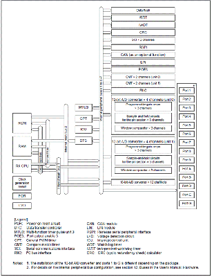
图1.RX62T方框图
This RSK is an evaluation tool for Renesas microcontrollers. This manual describes the technical details of the RSK hardware. The Quick Start Guide and Tutorial Manual provide details of the software installation and debugging environment.
RX62T RSK主要特性:
This RSK provides an evaluation of the following features:
• Renesas microcontroller programming
• User code debugging
• User circuitry such as switches, LEDs and a potentiometer
• Sample application
• Sample peripheral device initialisation code
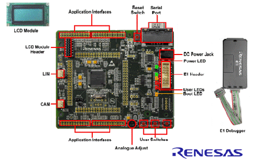
图2.RX62T RSK外形图
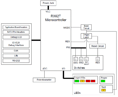
图3.RX62T RSK方框图
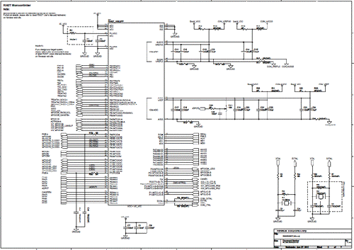
图4.RX62T RSK电路图(1)
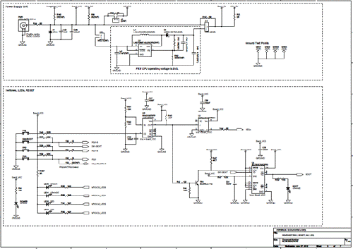
图5.RX62T RSK电路图(2)
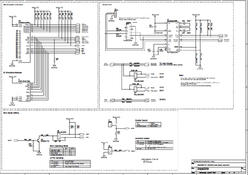
图6.RX62T RSK电路图(3)
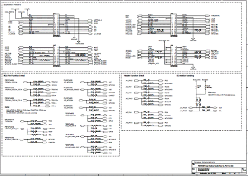
图7.RX62T RSK电路图(4)
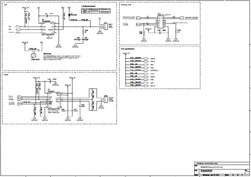
图8.RX62T RSK电路图(5)
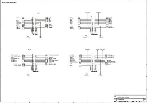
图9.RX62T RSK电路图(6)
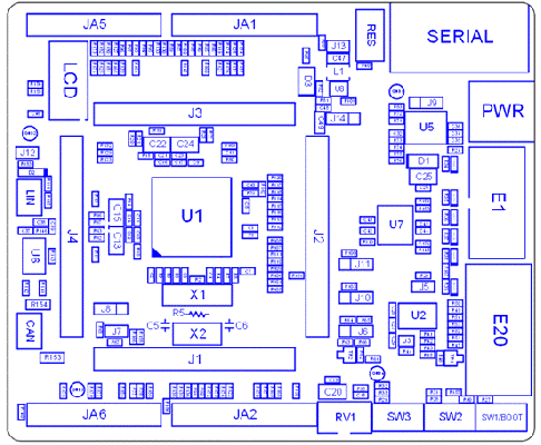
图10.RX62T RSK PCB元件布局图(顶层)
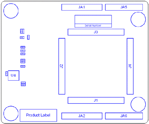
图11.RX62T RSK PCB元件布局图(底层)
|
|

