|

- UID
- 1023229
- 来自
- 中国
|

Xilinx 公司的Spartan-3AN FPGA系列把一流的低成本FPGA特性和非挥发技术组合在一起,有各种不同的密度,集成了存储器,乘法器,DCM,SelectIO,热插拔和电源管理等功能。Spartan-3AN FPGA的系统门从50K到1400K,等效的逻辑单元从1584到25344,Slice从704到11264,分布式RAM从11Kb到176Kb,块RAM从54Kb到576Kb,系统中闪存从1Mb到16Mb,而专用的乘法器从3个到32个,DCM从2个到8个,用户I/O从108个到502个,而差分I/O对从50对到227对,可以广泛应用在空间受到限制的地方如刀片服务器,医疗设备,汽车娱乐系统,远程信息处理,GPS和其它小型消费类电子产品。本文介绍了Spartan-3AN FPGA系列的主要特性以及入门开发板详细的电路图。
The Spartan-3AN FPGA family combines the best attributes of a leading edge, low cost FPGA with nonvolatile technology across a broad range of densities. The family combines all the features of the Spartan-3A FPGA family plus leading technology in-system Flash memory for configuration and nonvolatile data storage. The Spartan-3AN FPGA family is excellent for space-constrained applications such as blade servers, medical devices, automotive infotainment, telematics, GPS, and other small consumer products. Combining FPGA and Flash technology minimizes chip count, PCB traces and overall size while increasing system reliability. The Spartan-3AN FPGA internal configuration interface is completely self-contained, increasing design security. The family maintains full support for external configuration. The Spartan-3AN FPGA is the world’s first nonvolatile FPGA with MultiBoot, supporting two or more configuration files in one device, allowing alternative configurations for field upgrades, test modes, or multiple system configurations. Spartan-3AN主要特性:
The new standard for low cost nonvolatile FPGA solutions
Eliminates traditional nonvolatile FPGA limitations with the advanced 90 nm Spartan-3A device feature set
Memory,multipliers, DCMs, SelectIO, hot swap, power management, etc.
Integrated robust configuration memory
Saves board space
Improves ease-of-use
Simplifies design
Reduces support issues
Plentiful amounts of nonvolatile memory available to the user
Up to 11+ Mb available
MultiBoot support
Embedded processing and code shadowing
Scratchpad memory
Robust 100K Flash memory program/erase cycles
20 years Flash memory data retention
Security features provide bitstream anti-cloning protection
Buried configuration interface
Unique Device DNA serial number in each device for design Authentication to prevent unauthorized copying
Flash memory sector protection and lockdown
Configuration watchdog timer automatically recovers from configuration errors
Suspend mode reduces system power consumption
Retains all design state and FPGA configuration data
Fast response time, typically less than 100 μs
Full hot-swap compliance
Multi-voltage, multi-standard SelectIO™ interface pins
Up to 502 I/O pins or 227 differential signal pairs
LVCMOS, LVTTL, HSTL, and SSTL single-ended signal standards
3.3V, 2.5V, 1.8V, 1.5V, and 1.2V signaling
Up to 24 mA output drive
3.3V±10% compatibility and hot swap compliance
622+ Mb/s data transfer rate per I/O
DDR/DDR2 SDRAM support up to 400 Mb/s
LVDS, RSDS, mini-LVDS, PPDS, HSTL/SSTL differential I/O
Abundant, flexible logic resources
Densities up to 25,344 logic cells
Optional shift register or distributed RAM support
Enhanced 18 x 18 multipliers with optional pipeline
Hierarchical SelectRAM memory architecture
Up to 576 Kbits of dedicated block RAM
Up to 176 Kbits of efficient distributed RAM
Up to eight Digital Clock Managers (DCMs)
Eight global clocks and eight additional clocks per each half of device, plus abundant low-skew routing
Complete Xilinx ISE® and WebPACK software development system support
MicroBlaze and PicoBlaze embedded processor cores
Fully compliant 32-/64-bit 33 MHz PCI technology support
Low-cost QFP and BGA Pb-free (RoHS) packaging options
Pin-compatible with Spartan-3A FPGA family.

The Spartan-3AN FPGA architecture is compatible with that of the Spartan-3A FPGA. The architecture consists of five fundamental programmable functional elements:
Configurable Logic Blocks (CLBs) contain flexible Look-Up Tables (LUTs) that implement logic plus storage elements used as flip-flops or latches.
Input/Output Blocks (IOBs) control the flow of data between the I/O pins and the internal logic of the device. IOBs support bidirectional data flow plus 3-state operation. They support a variety of signal standards, including several high-performance differential standards. Double Data-Rate (DDR) registers are included.
Block RAM provides data storage in the form of 18-Kbit dual-port blocks.
Multiplier Blocks accept two 18-bit binary numbers as inputs and calculate the product. • Digital Clock Manager (DCM) Blocks provide self-calibrating, fully digital solutions for distributing, delaying, multiplying, dividing, and phase-shifting clock signals. A dual ring of staggered IOBs surrounds a regular array of CLBs. Each device has two columns of block RAM except for the XC3S50AN, which has one column. Each RAM column consists of several 18-Kbit RAM blocks. Each block RAM is associated with a dedicated multiplier. The DCMs are positioned in the center with two at the top and two at the bottom of the device. The XC3S50AN has DCMs only at the top, while the XC3S700AN and XC3S1400AN add two DCMs in the middle of the two columns of block RAM and multipliers. The Spartan-3AN FPGA features a rich network of traces that interconnect all five functional elements, transmitting signals among them. Each functional element has an associated switch matrix that permits multiple connections to the routing.
Spartan-3A/3AN FPGA Starter Kit Board

图1。Spartan-3AN FPGA入门开发板外形图
The Xilinx Spartan®-3A/3AN FPGA Starter Kit is invaluable to develop a Spartan-3A or Spartan-3AN FPGA application. The Spartan-3A/3AN Starter Kit board is ready for use, right out of the box. The design stored in external Flash exercises the various I/O devices, such as the VGA display and serial ports. In addition it demonstrates new FPGA features, such as selectable MultiBoot and the power-saving Suspend mode.
Spartan-3A/3AN FPGA入门开发板电路图
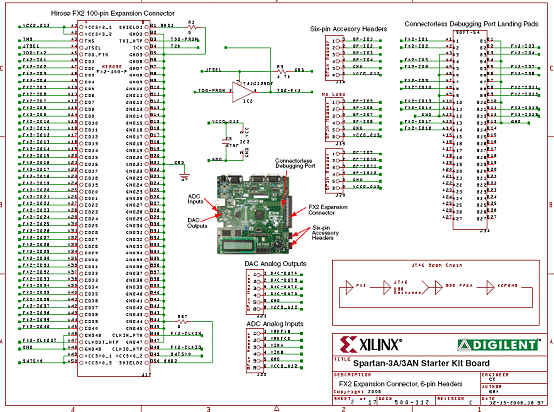
图2。Spartan-3AN FPGA入门板电路图(1)
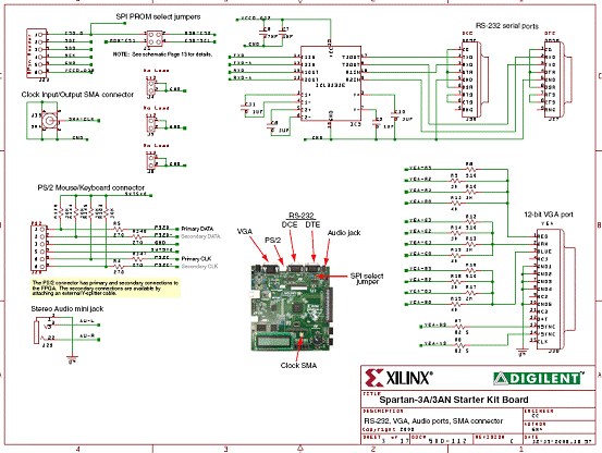
图3。Spartan-3AN FPGA入门板电路图(2)
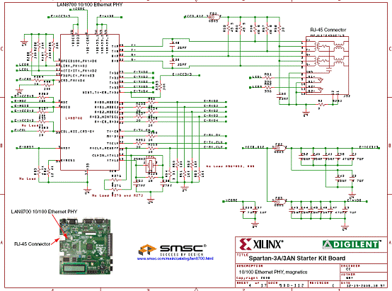
图4。Spartan-3AN FPGA入门板电路图(3)

图5。Spartan-3AN FPGA入门板电路图(4)
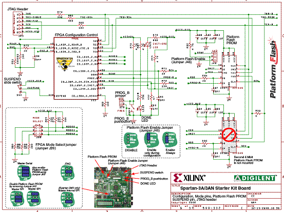
图6。Spartan-3AN FPGA入门板电路图(5)
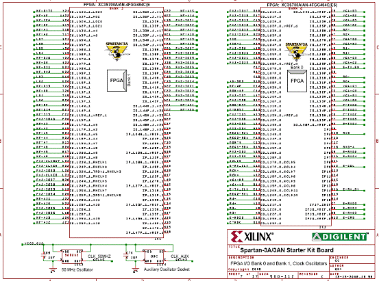
图7。Spartan-3AN FPGA入门板电路图(6)
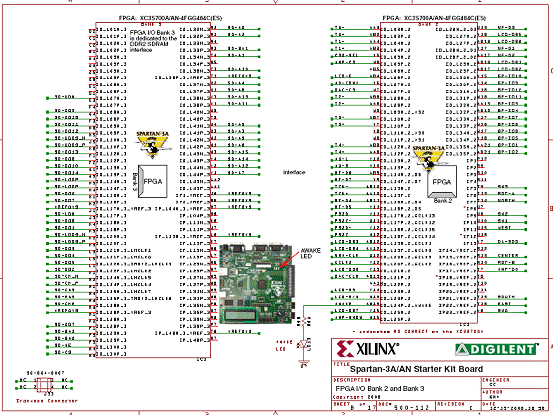
图8。Spartan-3AN FPGA入门板电路图(7)
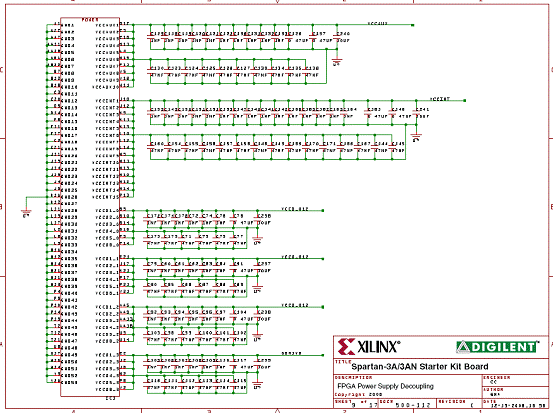
图9。Spartan-3AN FPGA入门板电路图(8)
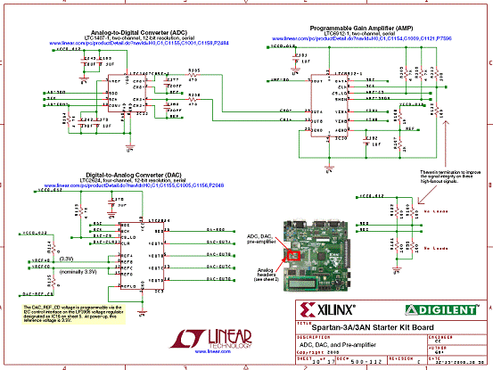
图10。Spartan-3AN FPGA入门板电路图(9)
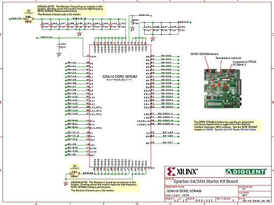
图11。Spartan-3AN FPGA入门板电路图(10)

图12。Spartan-3AN FPGA入门板电路图(11)
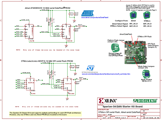
图13。Spartan-3AN FPGA入门板电路图(12)

图14。Spartan-3AN FPGA入门板电路图(13)

图15。Spartan-3AN FPGA入门板电路图(14)
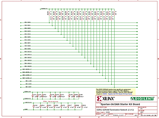
图16。Spartan-3AN FPGA入门板电路图(15)
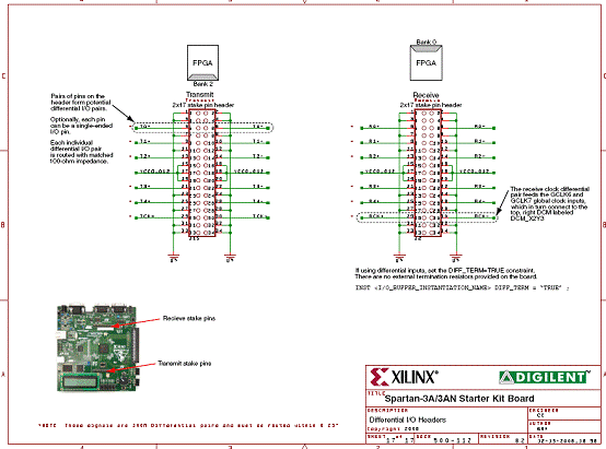
图17。Spartan-3AN FPGA入门板电路图(16)
详情请见:
http://www.xilinx.com/support/documentation/data_sheets/ds557.pdf
与
http://www.xilinx.com/support/documentation/boards_and_kits/ug334.pdf
和
http://www.xilinx.com/support/documentation/boards_and_kits/s3astarter_schematic.pdf |
|


