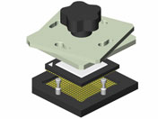
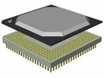
分球形出脚(SMT)和针形出脚两种设计.球形出脚的BGA插座系统主要适用于芯片的测试及开发等.该插座系统的特点是不用在PCB板上开孔,BGA插座的焊接方法和BGA芯片的焊接方法完全一样.同时如果在客户的目标板上BGA Pad旁边如果已经存在一些贴片器件而影响到BGA插座的安装,亦提供BGA插座的升高设计以便满足客户的实际要求.并可根据客户的BGA器件出脚,定制合适的BGA插座(Available for any chip size and grid pattern)。 产品特点:  Any package style: ceramic & plastic BGA, CSP, LGA, CGA, PSGA, MLF/QFN,QFP, SOIC, and other standard packages, custom packages or bare die
Inductance: less than 2nH Any package style: ceramic & plastic BGA, CSP, LGA, CGA, PSGA, MLF/QFN,QFP, SOIC, and other standard packages, custom packages or bare die
Inductance: less than 2nH
-1dB bandwidth: >14GHz for compression style; 3GHz for SMD style
available for any chip size and grid pattern
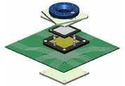
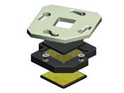
Same PCB layout as the IC (no holes required for SMD socket)
Minimal keepout area of 6mm beyond the IC’s periphery
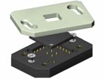
Raised SMD style for lifting socket over adjacent components
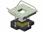
Low profile socket (standard Twist Lock is less than 10mm high with IC)
Contact force: max 40 grams per contact; lower forces available
Semi-custom design = lower cost and tailored to your needs http://www.lingmei.com.cn/procenter-bga.htm |